- 您现在的位置:买卖IC网 > Sheet目录214 > CM1213-08MR (ON Semiconductor)TVS ARRAY ESD PROT LO 8CH 10MSOP
CM1213
APPLICATION INFORMATION
Design Considerations
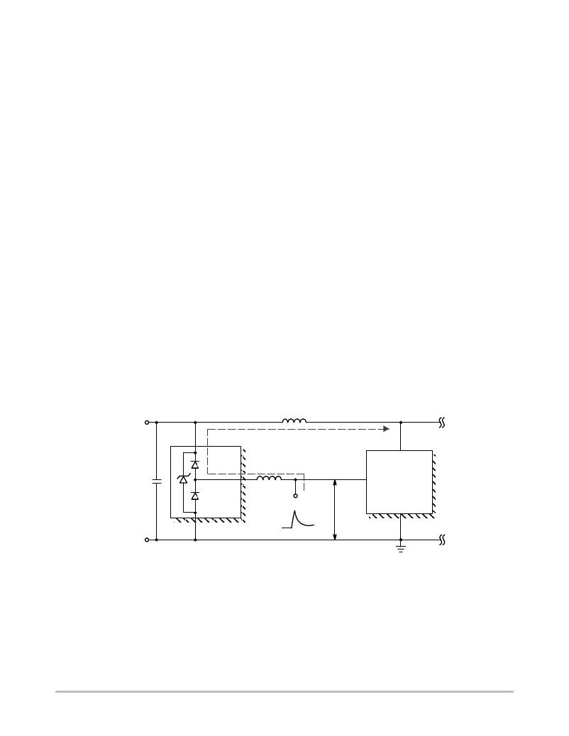
In order to realize the maximum protection against ESD pulses, care must be taken in the PCB layout to minimize parasitic
series inductances on the Supply/Ground rails as well as the signal trace segment between the signal input (typically
a connector) and the ESD protection device. Refer to Application of Positive ESD Pulse between Input Channel and Ground,
which illustrates an example of a positive ESD pulse striking an input channel. The parasitic series inductance back to power
supply is represented by L 1 and L 2 . The voltage V CL on the line being protected is:
V CL = Fwd voltage drop of D 1 + V SUPPLY + L 1 x d(I ESD ) / dt + L 2 x d(I ESD ) / dt
where I ESD is the ESD current pulse, and V SUPPLY is the positive supply voltage.
An ESD current pulse can rise from zero to its peak value in a very short time. As an example, a level 4 contact discharge
per the IEC61000 ? 4 ? 2 standard results in a current pulse that rises from zero to 30 Amps in 1 ns. Here d(I ESD )/dt can be
approximated by D I ESD / D t, or 30/(1x10 ? 9 ). So just 10 nH of series inductance (L 1 and L 2 combined) will lead to a 300 V
increment in V CL !
Similarly for negative ESD pulses, parasitic series inductance from the V N pin to the ground rail will lead to drastically
increased negative voltage on the line being protected.
The CM1213 has an integrated Zener diode between V P and V N . This greatly reduces the effect of supply rail inductance
L 2 on V CL by clamping V P at the breakdown voltage of the Zener diode. However, for the lowest possible V CL , especially when
V P is biased at a voltage significantly below the Zener breakdown voltage, it is recommended that a 0.22 m F ceramic chip
capacitor be connected between V P and the ground plane.
As a general rule, the ESD Protection Array should be located as close as possible to the point of entry of expected
electrostatic discharges. The power supply bypass capacitor mentioned above should be as close to the V P pin of the Protection
Array as possible, with minimum PCB trace lengths to the power supply, ground planes and between the signal input and the
ESD device to minimize stray series inductance.
Additional Information
See also ON Semiconductor Application Note, “Design Considerations for ESD Protection”, in the Applications section.
V P
L 2
POSITIVE SUPPLY RAIL
V CC
PATH OF ESD CURRENT PULSE I ESO
0.22 m F
D 1
ONE
CHANNEL
D 2 OF
CM1213
L 1
CHANNEL
INPUT
25 A
LINE BEING
PROTECTED
V CL
SYSTEM OR
CIRCUITRY
BEING
PROTECTED
V N
0A
GROUND RAIL
CHASSIS GROUND
Figure 5. Application of Positive ESD Pulse between Input Channel and Ground
http://onsemi.com
6
发布紧急采购,3分钟左右您将得到回复。
相关PDF资料
CM1214A-01SO
TVS AC SIGNAL ESD 1CH SOT23-3
CM1215-04SO
4 CH ESD ARRAY SOT23-6
CM1216-06MR
TVS ARRAY ESD LOW CAP 6CH 8MSOP
CM1220-08CP
TVS ARRAY ESD PROT 8CH 10CSP
CM1223-02SR
TVS ARRAY ESD LOW 2CH SOT143-4
CM1224-02SR
TVS ARRAY ESD LOW 2CH SOT143-4
CM1225-04DE
TVS ARRAY ESD LOW PROT 4CH 10DFN
CM1230-04CP
TVS ARRAY ESD LOW PROT 4CH CSP6
相关代理商/技术参数
CM1213-08MS
制造商:CALMIRCO 制造商全称:California Micro Devices Corp 功能描述:1, 2, 4, 6 and 8-Channel Low Capacitance ESD Protection Arrays
CM1213A
制造商:CALMIRCO 制造商全称:California Micro Devices Corp 功能描述:1-, 2- and 4-Channel Low Capacitance ESD Protection Arrays
CM1213A_11
制造商:ONSEMI 制造商全称:ON Semiconductor 功能描述:1, 2 and 4-Channel Low Capacitance ESD Protection Arrays
CM1213A-01SO
功能描述:ESD 抑制器 1-ch. 8KV/1pF Ultra RoHS:否 制造商:STMicroelectronics 通道:8 Channels 击穿电压:8 V 电容:45 pF 端接类型:SMD/SMT 封装 / 箱体:uQFN-16 功率耗散 Pd: 工作温度范围:- 40 C to + 85 C
CM1213A-02SO
功能描述:ESD 抑制器 2-ch. 8KV/1pF Ultra RoHS:否 制造商:STMicroelectronics 通道:8 Channels 击穿电压:8 V 电容:45 pF 端接类型:SMD/SMT 封装 / 箱体:uQFN-16 功率耗散 Pd: 工作温度范围:- 40 C to + 85 C
CM1213A-02SR
功能描述:ESD 抑制器 2-ch. 8KV/1pF Ultra RoHS:否 制造商:STMicroelectronics 通道:8 Channels 击穿电压:8 V 电容:45 pF 端接类型:SMD/SMT 封装 / 箱体:uQFN-16 功率耗散 Pd: 工作温度范围:- 40 C to + 85 C
CM1213A-04MR
功能描述:ESD 抑制器 4 CH LOW CAP ESD RoHS:否 制造商:STMicroelectronics 通道:8 Channels 击穿电压:8 V 电容:45 pF 端接类型:SMD/SMT 封装 / 箱体:uQFN-16 功率耗散 Pd: 工作温度范围:- 40 C to + 85 C
CM1213A-04S7
功能描述:ESD 抑制器 4-ch ESD Protection 8KV/1pF Capacitance RoHS:否 制造商:STMicroelectronics 通道:8 Channels 击穿电压:8 V 电容:45 pF 端接类型:SMD/SMT 封装 / 箱体:uQFN-16 功率耗散 Pd: 工作温度范围:- 40 C to + 85 C
